Within the vast realm of electronic components lies a powerful and versatile integrated circuit that has earned its place as an invaluable tool for engineers, hobbyists, and tinkerers alike. Encased within its unassuming package, the CD4027 offers a multitude of functionalities that unleash boundless possibilities for various electronic projects. With its reliable performance and ease of implementation, this dynamic integrated circuit has become an essential component in countless applications.
A beacon of innovation, the CD4027 boasts an intricate design that combines a multitude of capabilities in a single chip. By harnessing the power of advanced logic gates and flip-flops, it enables users to effortlessly manipulate and control voltages, signals, and data. Whether utilized in a digital clock, a binary counter, or an electronic switch, the CD4027 empowers engineers to design intricate circuits with remarkable precision and efficiency.
One of the CD4027’s standout features is its ability to provide a stable output under varying conditions, ensuring reliable performance even in the face of changing external factors. This reliability is achieved through robust internal circuitry that maintains precise timings and synchronization, resulting in consistent and accurate outputs. With this remarkable forethought, the CD4027 sets itself apart from other integrated circuits, making it a go-to choice for projects that require accuracy and dependability.
Join us on an exciting journey as we unravel the mysteries of the CD4027 datasheet, digging deep into its intricacies and shedding light on its vast array of capabilities. From learning how to decode its pin configuration and understanding the various components within, to exploring its vast repertoire of applications, this article aims to equip you with the knowledge and confidence to optimize the CD4027’s potential in your own electronic endeavors. Prepare to dive into this world of innovation and unleash your creativity with the limitless possibilities of the CD4027 integrated circuit!
DataSheet of CD4027: Functions, Features, and Pin Configuration

In this section, we will explore the various functions, features, and pin configuration of the CD4027 integrated circuit. The CD4027, also known as a complementary metal-oxide-semiconductor (CMOS) dual J-K master-slave flip-flop, offers a range of versatile capabilities and is widely used in electronic circuit designs.
Functions:
The CD4027 IC is primarily used as a binary counter and frequency divider. It provides an efficient way to count binary numbers and divide frequencies in electronic circuits. Additionally, it can be used as a toggle flip-flop or a data flip-flop, offering flexibility in circuit design.
Features:
One of the key features of the CD4027 is its low power consumption. It operates at a wide supply voltage range, making it suitable for various applications. The IC also has a wide input voltage range and excellent noise immunity, ensuring reliable operation in different environmental conditions.
Furthermore, the CD4027 offers edge-triggered flip-flop functionality and can handle high-speed operations. It has dual J-K inputs that allow both direct and complementary operation, providing designers with more options for circuit implementation.
Pin Configuration:
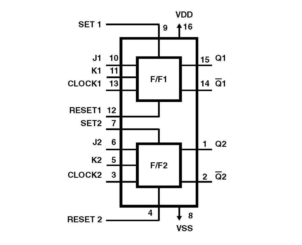
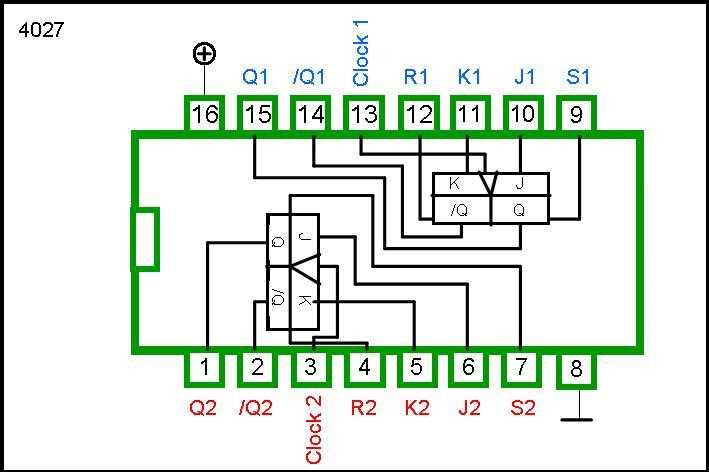
The CD4027 IC is encapsulated in a 16-pin dual in-line package (DIP) with its pins arranged in a specific configuration. Pin 1 and Pin 16 act as the power supply pins, with Pin 1 being the positive supply voltage (VDD) connection and Pin 16 being the ground (GND) connection.
Following the power supply pins, there are input pins such as J1, J2, K1, and K2, which are connected to the J and K inputs of the flip-flop. These pins allow for various input configurations, including parallel, serial, and combinational modes.
The output pins, denoted as Q and Q̅, represent the outputs of the flip-flop and can be connected to other components of the circuit for further processing or display.
Overall, understanding the functions, features, and pin configuration of the CD4027 is crucial for effectively incorporating this IC into electronic designs, enabling the realization of innovative and reliable circuits.
The Functions and Applications of CD4027
In this section, we will explore the various functions and applications of the versatile CD4027 integrated circuit. This IC offers a wide range of features and can be used in diverse electronic applications.
Functionality
The CD4027 is a dual J-K flip-flop that can operate in either the master-slave or toggle mode. It has two independent flip-flops with separate direct and complementary outputs. One of the key features of CD4027 is its ability to perform multiple functions with the help of external logic gates and control signals.
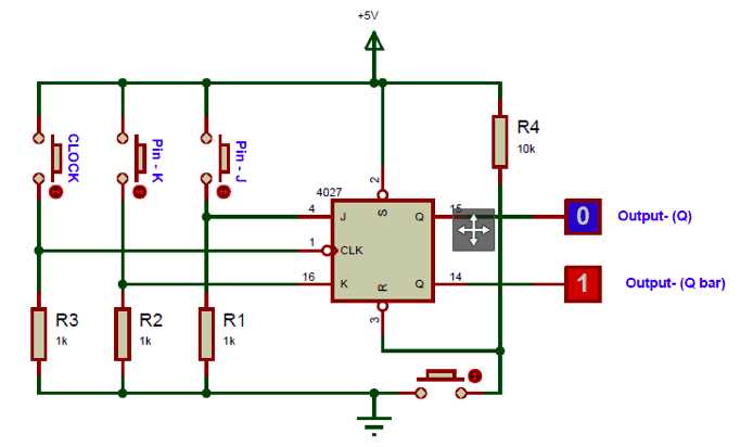
When used in the master-slave configuration, the CD4027 functions as a double-edge-triggered flip-flop that eliminates the possibility of false output due to race conditions. In the toggle mode, the IC can toggle its outputs based on the clock pulses it receives.
Applications
The CD4027 has a wide range of applications in the field of digital electronics. Some of its common uses include:
| Application | Description |
|---|---|
| Synchronous Counters | The CD4027 can be used to design synchronous counters that have multiple stages, enabling precise counting and control in various applications. |
| Frequency Division | By utilizing the toggle mode, CD4027 can divide the frequency of an input signal by two, making it useful in frequency division circuits. |
| Data Storage | Due to its flip-flop nature, CD4027 can serve as a basic building block for designing memory circuits that store data temporarily. |
| Real-time Clocks | With appropriate circuitry, CD4027 can be utilized in the creation of real-time clocks that accurately keep track of time. |
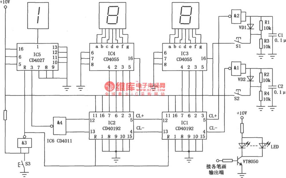
In addition to these applications, the CD4027 can be employed in various other digital systems, such as control systems, signal generators, and counters due to its flexibility, reliability, and ease of integration.
Overall, the CD4027 is a highly versatile integrated circuit that offers a range of functions and applications across different electronic devices and systems. Its flexibility and reliability make it a popular choice in the field of digital electronics.
Pin Configuration and Operating Parameters of CD4027
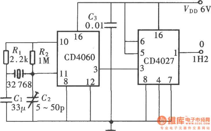
The pin configuration and operating parameters of the CD4027 integrated circuit provide crucial information for understanding its functionality and utilizing it effectively in electronic circuits. This section will provide an overview of the various pins and their functions, as well as the operating parameters that define the device’s performance characteristics.
Starting with the pin configuration, the CD4027 features a total of 16 pins, each serving a specific purpose in the circuit. These pins include power supply pins, input pins, output pins, and control pins. Each pin is identified by a unique name or label, enabling easy identification and connection within a circuit.
The power supply pins include VDD and VSS, which provide the necessary voltage levels for the proper functioning of the CD4027. These pins should be connected to the appropriate power sources to ensure stable operation. It is essential to follow the manufacturer’s specifications and guidelines regarding voltage levels and power supply connections.
The input pins, labeled as A, B, C, and D, serve as the inputs for the CD4027. These pins receive the binary inputs that determine the desired functionality or logic operation of the device. Connecting these pins correctly is crucial for achieving the desired results.
The outputs of the CD4027 are labeled as Q and /Q. The Q output represents the normal output state, while the /Q output represents the complement or inverse of the Q output. These outputs are typically connected to other components or circuits to achieve the desired logical operations or functional outputs.
Along with the input and output pins, the CD4027 features control pins that provide additional functionality and control over the device. These control pins include the clock pin (CK), the reset pin (R), and the set pin (S). These pins allow for synchronization, resetting, or presetting of the device to achieve specific functions or trigger operations as required.
Moving on to the operating parameters of the CD4027, these define the device’s performance characteristics and ensure reliable operation. The parameters include operating voltage range, supply current, operating temperature range, propagation delay, and output voltage levels. Understanding and adhering to these operating parameters is critical for achieving optimal performance and preventing damage to the device.
In conclusion, the pin configuration and operating parameters of the CD4027 play a vital role in its successful integration and utilization in electronic circuits. Understanding the various pins’ functions and correct connections, as well as adhering to the operating parameters, ensures reliable and efficient performance of the device in various applications.