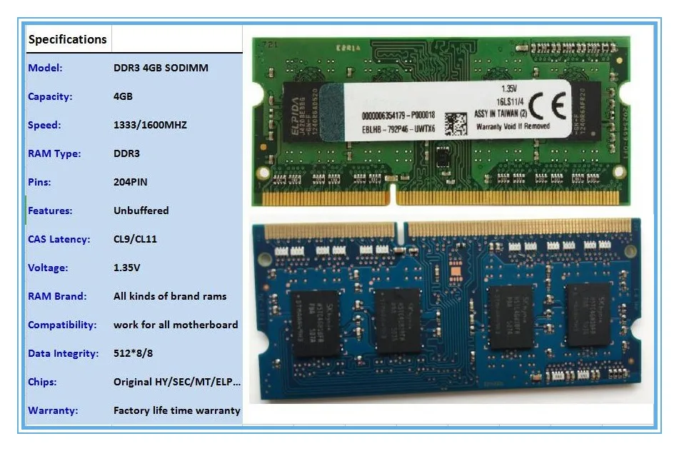
Imagine a world where information flows seamlessly, where devices respond instantaneously to every command. A world where data transfer is swift and efficient, allowing for the smooth operation of our technological ecosystem. Welcome to the world of Synchronous Dynamic Random-Access Memory (SDRAM), a marvel of modern computing.
In this article, we delve into the intricacies of SDRAM, unravelling its inner workings and shedding light on its significance in the realm of electronics. Explore with us as we navigate through the labyrinth of this essential component, gaining insights into its role in memory storage, data retrieval, and overall system performance.
Prepare to be captivated as we embark on a journey through the mesmerizing world of SDRAM, an integral part of our digital landscape. Brace yourself for an exploration filled with technical prowess and innovation, as we uncover the secrets behind this dynamic piece of technology.
The Basics of Sdram Technology
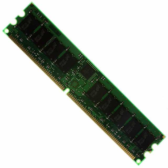
In today’s digital age, efficient and high-speed data storage and retrieval have become crucial for various electronic devices and systems. One technology that plays a vital role in achieving these goals is Sdram. Understanding the fundamentals of Sdram technology is essential for grasping its importance in modern computing and its widespread implementation across a range of industries.
Essentially, Sdram is a type of dynamic random-access memory (DRAM) that uses synchronous signaling to improve data transfer speed and efficiency. Unlike its predecessor, asynchronous DRAM, Sdram synchronizes the memory controller with the memory module to ensure precise and timed data transfers. It eliminates the need for continuous refreshing of data, enabling faster and more efficient access to stored information.
One of the key advantages of Sdram technology lies in its high data transfer rates. By synchronizing the memory controller and memory module, Sdram allows for simultaneous data transmission on both rising and falling edges of the clock signal. This double data rate (DDR) capability effectively doubles the data transfer rate compared to traditional DRAM, making it ideal for memory-intensive applications such as video streaming, gaming, and multitasking.
Another crucial aspect of Sdram technology is its capacity for storing a large amount of data. With the advancement of technology, Sdram has evolved to offer higher densities, allowing for greater memory capacity in increasingly compact form factors. This enables devices to handle vast amounts of data and run resource-intensive applications seamlessly, contributing to enhanced user experiences and improved overall system performance.
Furthermore, Sdram technology also ensures reliability and data integrity. By utilizing error-checking and correction (ECC) techniques, Sdram can detect and correct errors that may occur during data transmission or storage. This feature is particularly valuable in critical applications where data accuracy and integrity are of utmost importance, such as server systems, scientific research, and financial institutions.
In conclusion, Sdram technology offers numerous advantages in terms of speed, capacity, and reliability, making it a crucial component in modern computing. Its synchronous signaling, high data transfer rates, and large memory capacity make it a preferred choice for a wide range of applications. As technology continues to advance, further innovations in Sdram technology are expected, promising even greater performance and efficiency in the future.
Key Features and Specifications
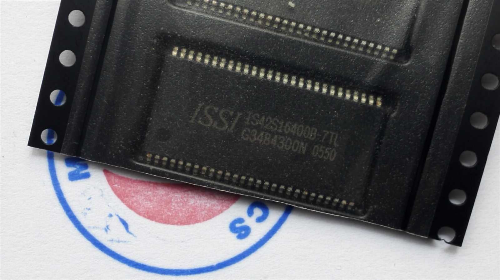
Discover the outstanding characteristics and specifications of the cutting-edge SDRAM technology, providing unparalleled performance and reliability for various applications. This section highlights the key features and specifications that make SDRAM the preferred choice for high-speed data storage and retrieval.
Innovative Performance

Experience lightning-fast data access and transfer speeds with SDRAM’s advanced architecture, engineered to deliver unparalleled performance in handling large amounts of data efficiently. With its revolutionary design, SDRAM ensures seamless multitasking and enhanced system responsiveness, enabling smooth and uninterrupted operations even in the most demanding computing environments.
Reliable and Stable Operation
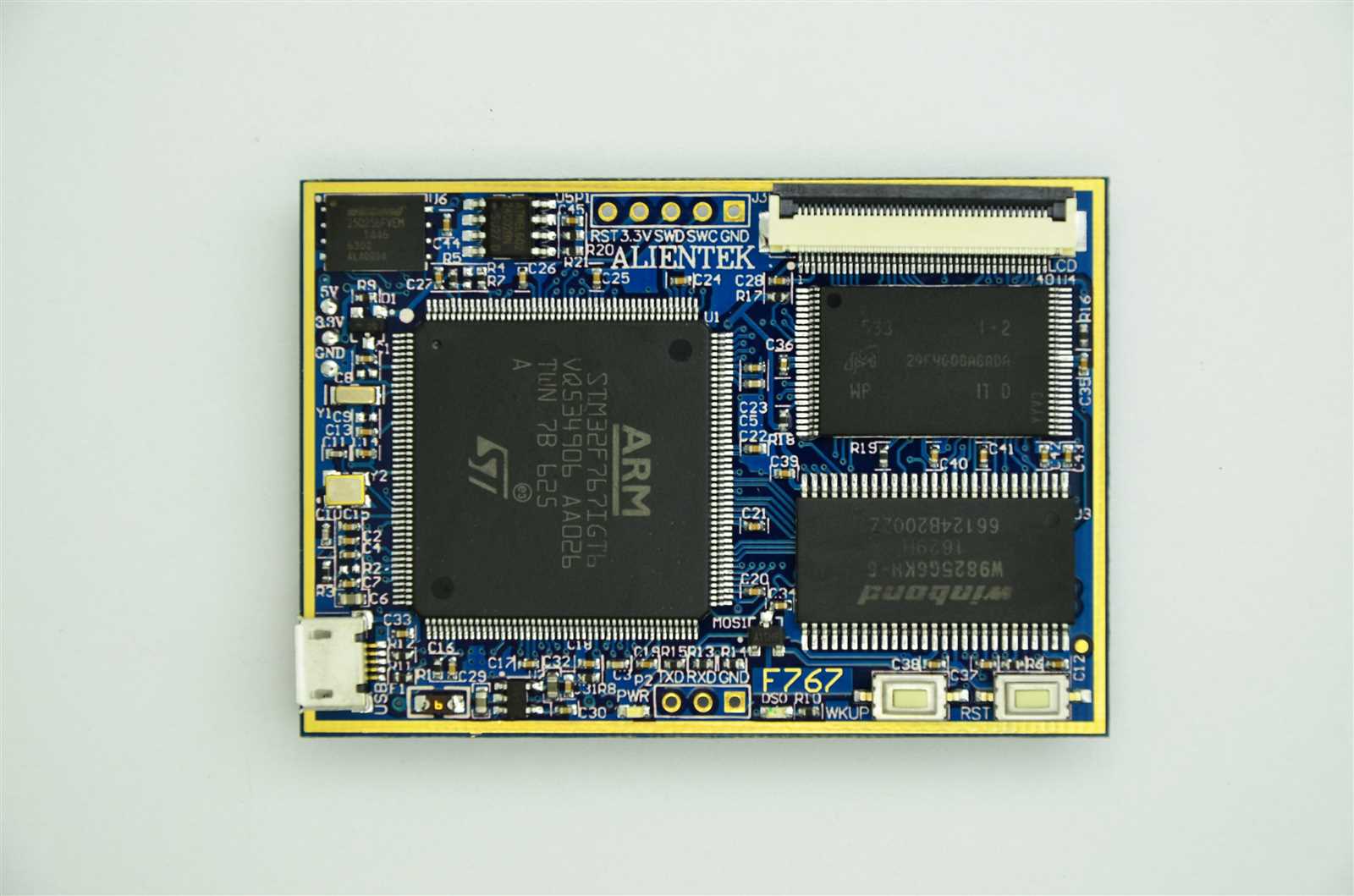
Benefit from SDRAM’s exceptional reliability and stability, ensuring consistent and error-free data storage and retrieval. SDRAM’s robust design and stringent manufacturing processes guarantee the highest level of quality and durability, making it the ideal choice for critical applications that require continuous and reliable operation. Whether utilized in enterprise servers, networking equipment, or consumer electronics, SDRAM provides the peace of mind that data will be securely stored and rapidly accessed.
Clock Frequency and Timing Signals
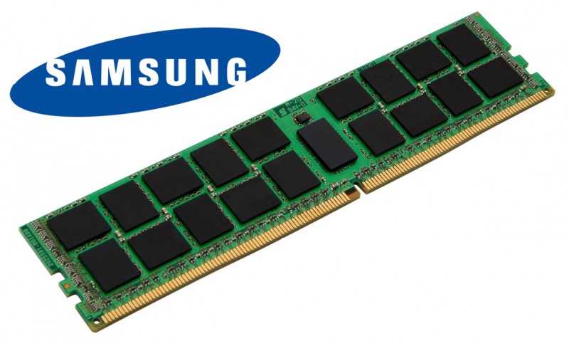
The section explores the importance of clock frequency and timing signals in relation to SDRAM technology. The efficient operation of SDRAM relies heavily on precise synchronization and timing control, which are achieved through clock frequency and timing signals.
Key Factors in Clock Frequency
The clock frequency determines the speed at which data can be transferred in and out of the SDRAM. A higher clock frequency allows for faster data transfer rates, resulting in improved overall system performance. It is crucial to understand the relationship between clock frequency and SDRAM capabilities to optimize the usage and maximize the performance of the memory device.
Timing Signals and Responsiveness
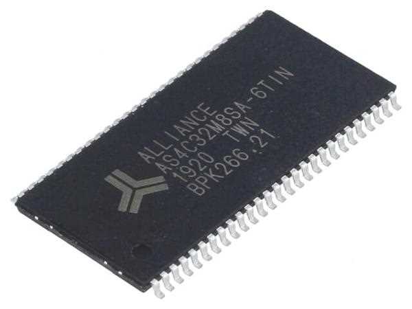
Timing signals play a significant role in ensuring accurate data transfers and preventing data corruption or loss. These signals synchronize the actions of various components within the SDRAM, facilitating the orderly execution of read and write operations. Proper timing control guarantees data integrity and responsiveness, enabling seamless interaction between the SDRAM and the rest of the system.
Timely and synchronized clock frequency and timing signals are vital for the optimal functioning of SDRAM technology. The efficiency of data transfers and overall system performance heavily relies on precise timing control. Understanding the significance of clock frequency and timing signals allows for the effective utilization and enhancement of SDRAM capabilities in various applications.
Addressing Modes and Burst Length
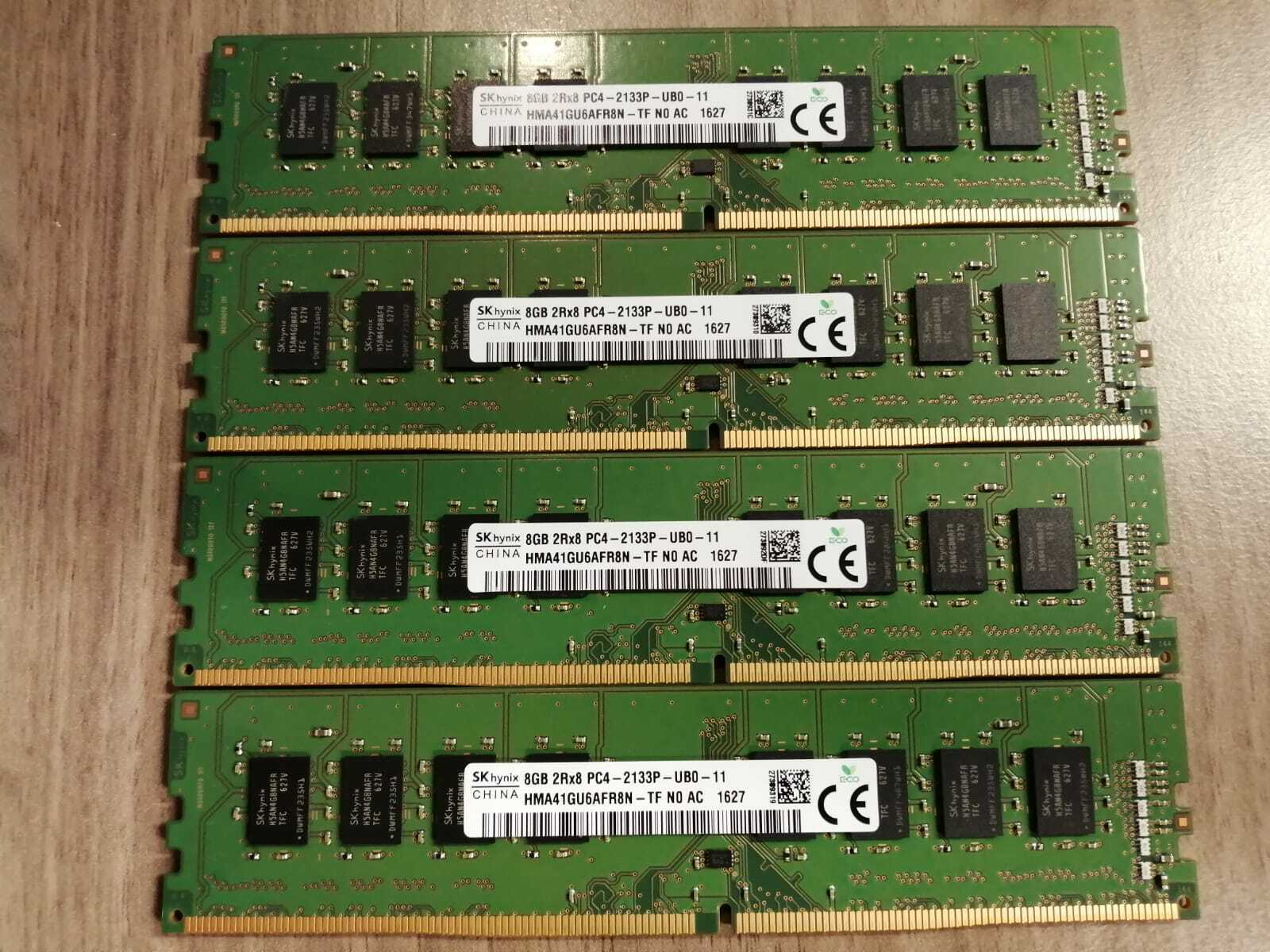
In the realm of memory architecture, the way data is accessed and transferred plays a crucial role in maximizing the performance of a system. Addressing modes and burst length are two integral concepts in understanding the efficiency of SDRAM operation without delving into the specifics of a datasheet.
Addressing modes refer to the various methods employed by SDRAM to locate and access specific data stored in its memory cells. Different addressing modes offer different benefits and trade-offs, enabling flexibility in accessing data based on specific requirements. By utilizing a combination of addressing modes, SDRAM can efficiently retrieve data, facilitate complex operations, and minimize latency.
Burst length, on the other hand, pertains to the number of sequential data transfers that occur between the SDRAM and the memory controller in a single access command. It determines the amount of data that can be transferred during a burst cycle. Burst length plays a crucial role in enhancing data transfer rates and reducing the overhead associated with accessing individual data items.
- Sequential Burst Length: This mode enables the transfer of data in a sequential order, allowing for faster data retrieval and reduced latency. It is particularly useful for applications that require contiguous data, such as multimedia streaming or graphics rendering.
- Interleaved Burst Length: In this mode, data is transferred in an interleaved manner across multiple banks within the SDRAM. It allows for parallel data access and improved overall throughput.
- Wrap Burst Length: This mode enables the data transfer to wrap around within a burst cycle, allowing for efficient access to multiple data points without the need for additional command operations.
By understanding the various addressing modes and burst lengths supported by SDRAM, system designers can optimize the memory performance for their specific applications. Choosing the appropriate combination of addressing modes and burst lengths can greatly enhance the efficiency and speed of data access, resulting in improved overall system performance.
Pin Configuration and Signal Groups

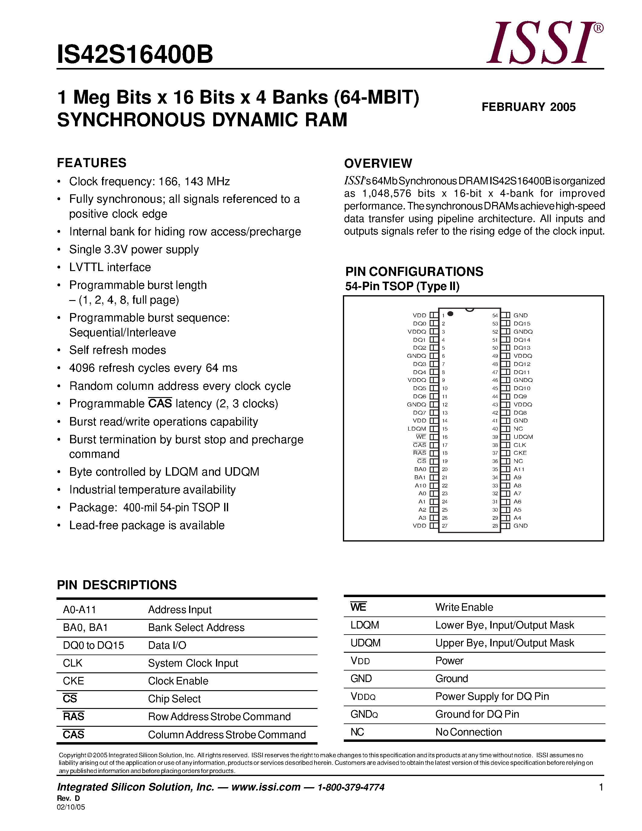
The pin configuration and signal groups of the Sdram play a crucial role in understanding the communication and functionality of this memory device. By examining the arrangement and organization of the pins, we can gain valuable insights into how different signals are grouped and their specific roles in the Sdram operation.
Primary Signal Group
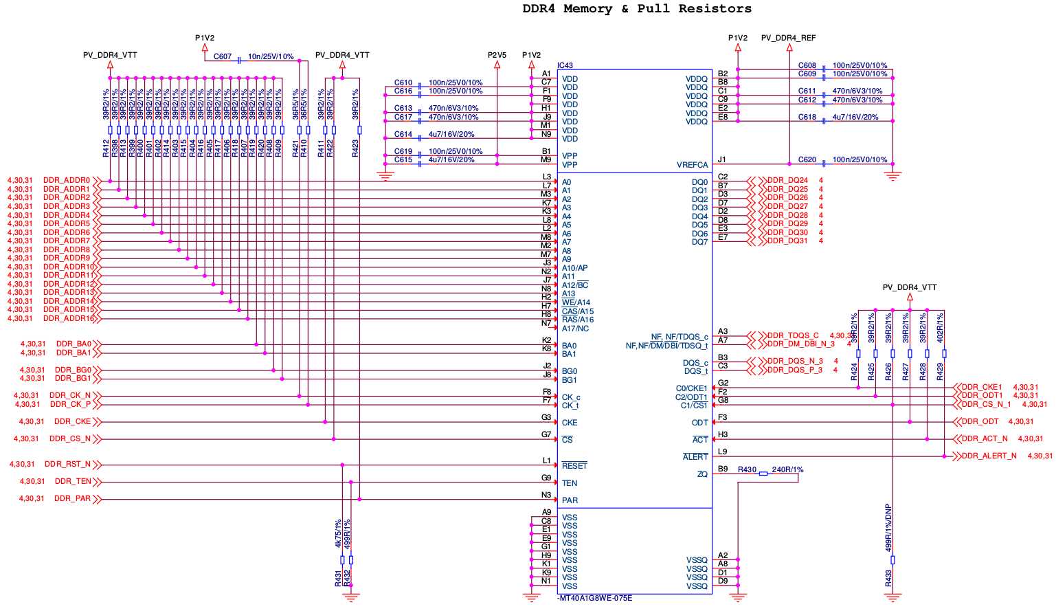
The primary signal group consists of essential signals that are vital for the basic functioning of the Sdram. These signals include the power supply, clock input, and ground connections. The power supply pins provide the necessary voltage levels required for the operation of the device, while the clock input signal synchronizes the data transfer and processing. Ground connections ensure a stable reference potential for accurate signal transmission and reception.
Data and Control Signal Group
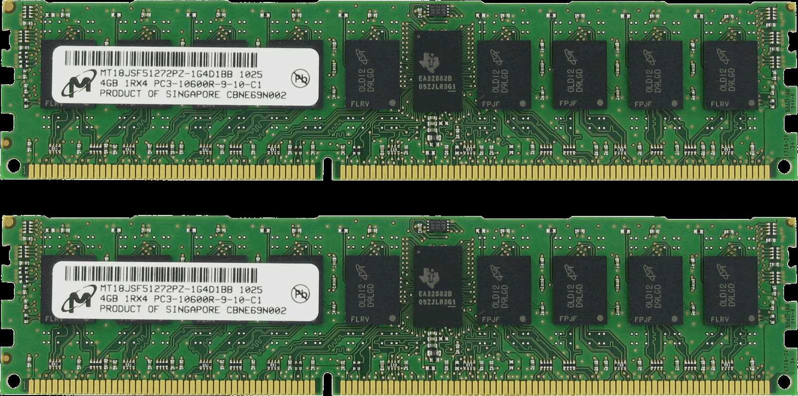
The data and control signal group in the Sdram is responsible for the actual data transfer and control operations. It includes signals such as data input, data output, address inputs, and control inputs. The data input pin is used for transferring data into the memory, while the data output pin allows the retrieval of stored data. The address pins determine the location where data is stored or read from, and the control inputs manage various operations such as read/write control and command execution.
| Pin Name | Description |
|---|---|
| Data Input/Output (DQ) | Bi-directional pins for data transfer |
| Address (A0-Ax) | Input pins for specifying memory locations |
| Control (C0-Cx) | Input pins for controlling Sdram operation |
This table provides a summary of some of the important pins and their descriptions within the data and control signal group. These pins are crucial for establishing communication and are necessary for proper Sdram functioning.